First ESA qualification granted for High Density Interconnect PCBs
A printed circuit board (PCB) manufacturer ACB, in Belgium, has been granted both a company and technology-based ESA qualification for their High Density Interconnect Printed Circuit Boards for the first time.
The road to qualification was full of technical challenges as this advanced PCB technology is complex to manufacture and the failure modes are notoriously difficult to screen. Microprocessor chips and other EEE components do not function in isolation. They need to be interconnected, as well as protected from harsh environmental conditions caused by soldering processes, ground-based testing, launch and prolonged operation in space. Back-end packaging of chips as well as system level packaging when assembling EEE parts on PCBs makes up the nerves and the veins of the electronic system, connecting the brains – the instruments – through signals and power. The packaging technologies provide the robustness for the system’s sensitive EEE parts, which need reinforcement and protection from mechanical and thermal stress to operate reliably and in unison within the electronic system.
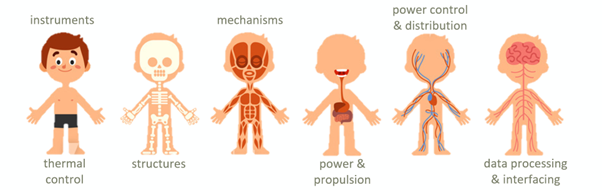 +
+Figure 1 Anatomy of a spacecraft
Developments at chip level have a profound impact on its packaging, PCB and electronic assembly technologies. Most prominently, the high number of component input and outputs, their small pitch and high signal speeds drive the need for short, dense and complex routing technologies in the PCB assembly. These High Density Interconnect (HDI) technologies were so far not covered by the generic PCB qualification scheme as per ECSS-Q-ST-70-60. This required case-by-case project qualification of individual designs and batches -- a significant hurdle in space projects.
A specific technology feature of HDI PCBs are microvias. These are laser-drilled holes in the dielectric insulator that expose the underlying internal copper layer. Subsequent plating processes ensure connectivity between layers. The adhesive bond between copper plating and the internal layer depends, among other things, on the efficiency of wet chemistry and plasma gas processes to clean the surface in the small diameter blind holes, which typically includes dozens of process steps and hundreds of parameters. This is inspected and tested on a relatively small sample size and it is critical that the same efficiency is ensured on the thousands of microvia holes in the PCB, on every production panel of every batch and every design. A potential weakness is likely to manifest itself only in hot conditions as the plated copper pulls away from the internal layer. When diagnostics are run at room temperature, such failure may self-heal and remain undetected. Qualitative inspection using microscopy is also inefficient, as the polishing on soft copper can mask a crack line and only very few holes can be assessed using such labour intensive procedure. The difficulty to screen for this failure mode has given rise to a global industry alert, named ‘the hidden reliability threat’ and is subject of extensive technical sessions in conferences on electronics manufacturing and packaging.
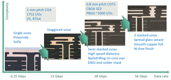 +
+Figure 2 HDI PCB technology roadmap
During the contract it turned out that other HDI features, named buried vias, are more prone to thermal cycling fatigue than the microvias. The latter were already subject to several process optimisations and the same exercise needed to be done for the buried via. The qualification was declared failed due to copper crack initiations. After optimisation of design and processes, supported by modelling and a design of experiments, the qualification vehicle was redesigned, remanufactured and retested and successfully awarded.
The activity was funded through the General Support Technology Programme’s (GSTP) Element 1. The Belgian consortium, which ACB was a part of, was led by IMEC and included TAS-B. The activity was described in the Advanced Manufacturing compendium and awarded in Belgium in 2018. Several workshops and review meetings were held, not only within the consortium but also to include input from external stakeholders and the possible OEM customer base. Five papers were published in various conferences and journals, such as the CEAS space journal . The consortium members received the best international paper award in the world’s most prominent conference IPC APEX EXPO 2020, as well as an honourable mention in 2022. The activities and published results led to a strengthened collaboration with world’s leading experts in HDI technology. Recently, the global electronics industry association IPC raised a European working group to further investigate microvia reliability, which is led by ESA and IMEC.
A similar GSTP activity on HDI is about to be concluded with two French PCB manufacturers, and another one will be initiated this year in Italy. Moreover, IMEC and ACB have recently kicked off a follow-on activity for High Speed HDI, which aims to further improve the routing technology for better signal integrity, as well as a dedicated activity on thermomechanical modelling of electronic modules. Meanwhile, TESAT pursued an internal technology development and qualification activity for High Speed HDI which is about to be concluded as well. In generic terms, the European PCB supply chain is under tremendous pressure to provide cost-effective high-reliability and high-end technologies in a short lead-time. Technology development contracts are paramount to spin-in advanced PCB technologies in ESA projects. The up-to-date status of qualified PCB technology can be found on ESCIES.org.