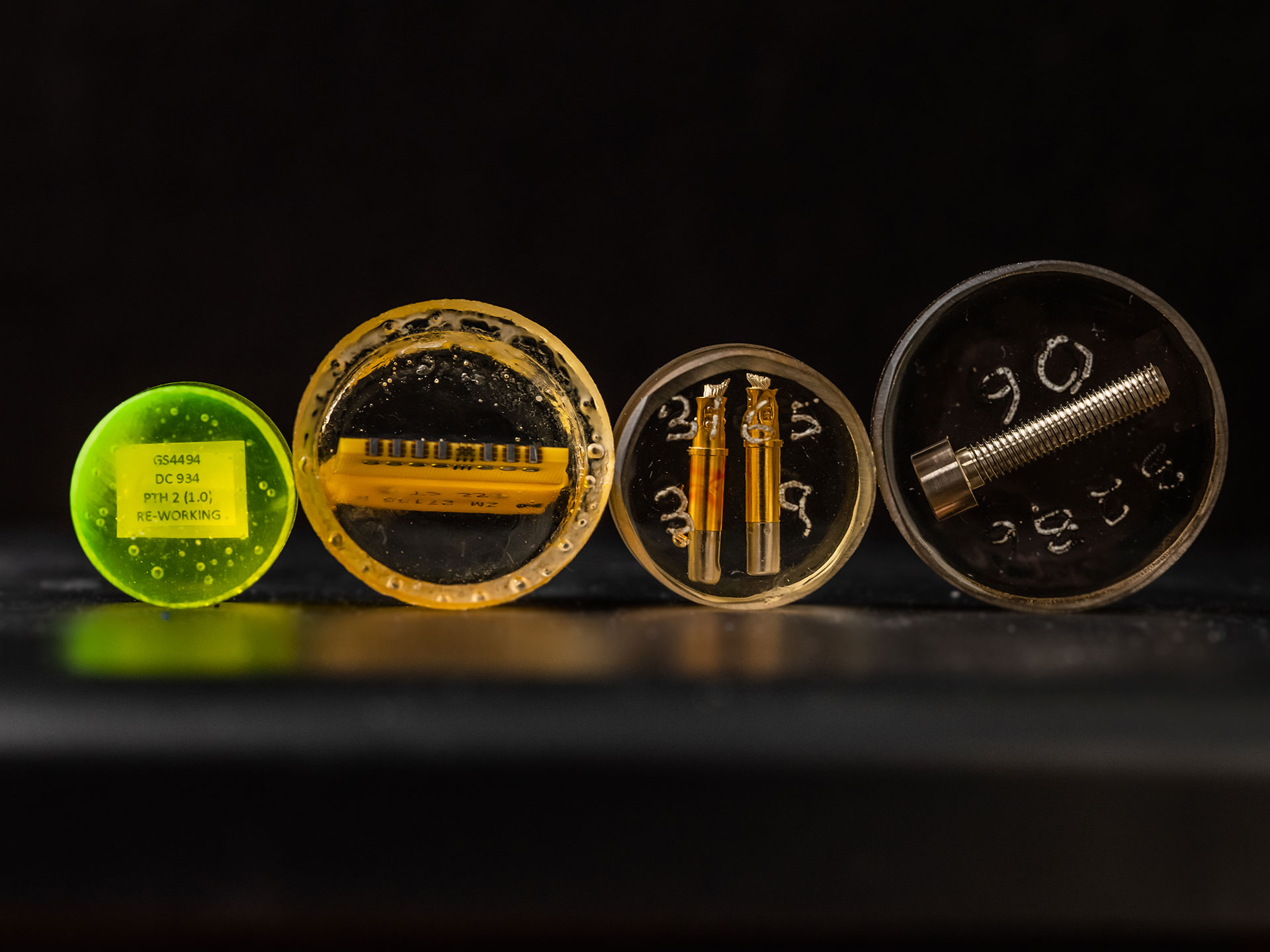
Discs for Fault Detection
Embedded within these resin discs are vital clues to determine whether future space missions will fail or thrive.
These are microsections taken from printed circuit boards (PCBs) and other parts, being considered for use by coming ESA projects. Such elements are key building blocks of space missions.
As their components become smaller, spacecraft are becoming much smarter and more capable – provided of course that the parts work as they are supposed to.
ESA’s Materials and Electrical Components Laboratory is tasked with checking if the performance and workmanship of candidate parts meet rigorous space-quality standards. Any defect in the parts (or in the soldering process used to attach components to PCBs) could impair spacecraft, or even lead to the total loss of a mission.
For its role as technical gatekeeper, the Lab is equipped with powerful diagnostic tools, including optical and scanning electron microscopes. The microsections are cast inside resin at ESTEC to make them easier to grind, polish and inspect under a microscope. In some cases, fluorescent dye is added to help detect defects – it fills cracks when the sample is initially cased in resin so that engineers can see that the defects were not caused in the preparation of the sample.
This image is one of the 99 Objects of ESA ESTEC website, a set of intriguing, often surprising artefacts helping tell the story of more than half a century of activity at ESA’s technical heart.

A selection of objects in resin before testing. Credit: ESA-Remedia

