Data Systems and Microelectronics Laboratory
The Data Systems and Microelectronics Laboratory is a joint undertaking across the Microelectronics Lab and the On-Board Computers and Data Handling Lab
The Data Systems and Microelectronics Laboratory encompasses the Data Handling System (DHS) and Microelectronics laboratories. The DHS laboratory focuses on the On-Board Platform / Payload Data Handling and Processing disciplines. While the Microelectronics laboratory covers all aspects of the microelectronic discipline necessary to support ESA projects.
The DHS laboratory boasts multiple Data Handling facilities supporting related R&D engineering tasks. The laboratory aims at promoting open collaboration founded on sharing information, experiences and facilities as part of the larger Avionic system domain. The Laboratory collaborates with ESA’s Control, Data and Software Systems divisions, enabling the assessment of new avionics technologies for the benefit of both ESA and European industry. In particular, Data Handling System concepts can be demonstrated on the available Test Benches, with their access considered beneficial for small and medium sized enterprises. The DHS laboratory is a strategic resource providing independent assessments of various DHS topics in support of ESA programs and European industry.
The Microelectronic laboratory maintains several facilities covering semiconductor processes and design kits, ASIC and FPGA development tools that allow support of the end-to-end development of complex space microchips and their building blocks. This laboratory also strongly supports the ESA IP Cores Service. The laboratory mainly conducts engineering tasks but also assists in direct project support activities. Microelectronics is a transversal domain supporting numerous R&D activities originating from other technology disciplines.
For testing requests, access to lab facilities, training and consultancy services, please refer to:

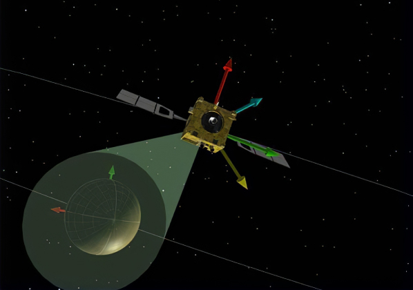 +
+EuroSim
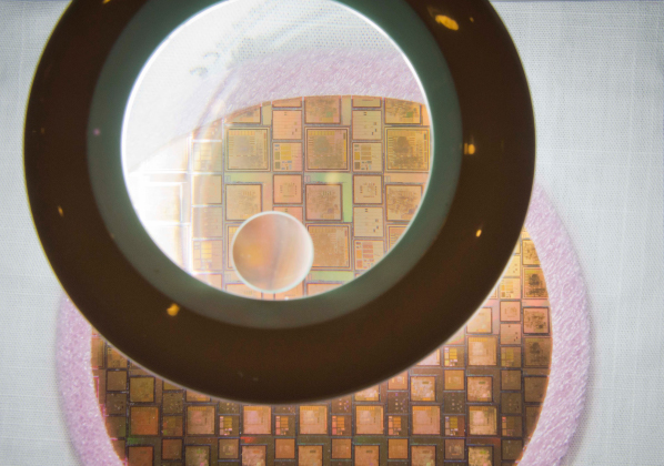 +
+Integrated circuits on silicon wafer
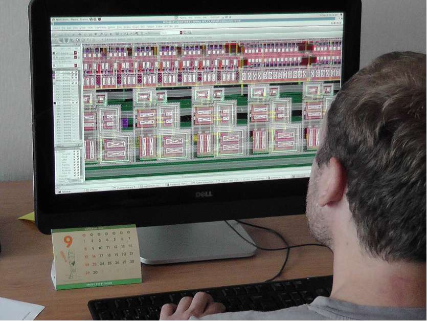 +
+Layout of Single Event Transient Test Chip using DARE180 IMEC technology undergoing design at Microelectronics Lab
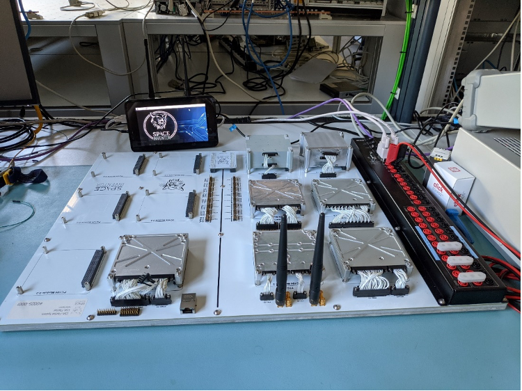 +
+Cubesat Test-Bed
ESA IP Cores
The ESA IP Cores Service and its catalogue of existing and under-development new ESA IP Cores is technically maintained with the infrastructure of the Microelectronics Lab. It provides with ASIC and FPGA building blocks to all ESA projects and R&D activities needing any of these IP Cores.
Services
Testing
- Performance evaluation
- Qualification & validation
- Test beds development
- Test methods development
- Anomaly investigations
- Characterisation
- Fault injection tests to emulate radiation effects in ASICs and FPGAs
Technical Expertise
- Consultancy
- Training
- Ad hoc auditing
- Development of Space Standards
- Complex IC or IP Cores anomaly investigations
Simulation
- Modelling
- Virtual Simulation
- Modelling and simulation of complex IC in various abstraction levels: 3D layout, transistor level, RTL, behavioral
- Modelling languages: VHDL, Verilog, System Verilog, SystemC
- Protocols simulation

WE CAN HELP YOU GET THE BEST OUT OF OUR LABORATORIES
FOR FURTHER INFORMATION REGARDING THE ACCESS TO THE LABORATORY
Contact us via Email